To be able to speed-up high-resolution ΣΔ ADC design, Axiom IC has developed an ADC concept that relies heavily on digital signal processing together with a special multibit D/A converter in the feedback path. This DAC is silicon-proven, well characterized and easy to port or modify (see SDCRDAC24bHBW datasheet).
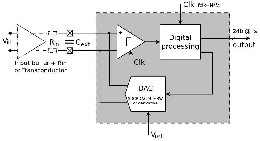
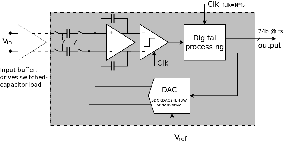
The ADC concept was initially developed for bandwidths of 5/10/20kHz, and SNR ratios of 110dB-120dB, with 24bit outputs. However, the system can easily be dimensioned for other bandwidths or SNR values. Two implementation variants are shown in figure 1 and 2, with the gray area marking the contents of the proposed ADC's.
Both ADC's use Axiom's SDCRDAC24bHBW IP block as DAC, as this sigma-delta DAC has proven itself in other applications with low signal frequencies. It is temperature stable, has very low 1/f noise and a high resolution.
Additional components needed to make an ADC are a first-order analog filter, comparator and digital signal processing. Due to the low signal frequencies, chopping will be used inside the ADC, to remove offset and 1/f noise.
The two ADC variants differ in how the analog filter is implemented. It can be either implemented as a passive filter with a Cext in the order of 10nF or higher (so probably external), or with an on-chip active filter
Two variants of this design are shown on the right.


Active filter ADC (variant 1)
This ADC mostly resembles a traditional sigma-delta structure, as it uses an active integrator as a loop-filter (which adds one order of noise-shaping. Higher-order noise-shaping is done in the digital domain). With this setup, the system can interface with switched-capacitor, sampled front-ends. It the input is continuous-time, then an input-buffer is needed to charge the switched-capacitor input load at the input sample rate (5 MHz) with enough settling (e.g. >12tau). Note that, Axiom can also take care of the design of the input buffer, with which Axiom has plenty experience.
Amplifier-less ADC (variant 2)
The second type of ADC ommits active filtering altogether, further reducing the number of analog parts that have to be designed/integrated. Instead, the filtering is done with an external RC filter. An advantage of the passive filter in the implementation in figure 2 is the relaxed requirements for the input buffer (which can be either a voltage buffer that drives Rin or can be a transconductor in which case Rin can be omitted).
The SDCRDAC24bHBW is a differential DAC (DM-DAC), but with some additional circuits, the ADC is able to convert both differential as well as single-ended input signals. The input resistors (Rin) determine the input voltage range, which can thus be rail-to-rail (but also outside the supply rails or referenced to 'true-ground' when that is of interest).
The output of the ADC can be made available either as a bitstream at the clock rate (or the clock rate e.g. fclk/4), for a simple one-wire data interface (with filtering of the bitstream done later in the signal chain), or it can be down-sampled internally to a lower rate and made available as PCM code.
Next to the feedback DAC, the number of analog components in the ADC can be kept to a minimum, enabling fast, low-risk implementation cycles. It is even possible to build ADC demonstrators with the existing DAC IP, to further increase confidence prior to tape-out.